

© Semiconductor Components Industries, LLC, 2011
October, 2011 − Rev. 8
1 Publication Order Number:
MMDF2C03HD/D
MMDF2C03HD
Power MOSFET
2 Amps, 30 Volts
Complementary SO−8, Dual
These miniature surface mount MOSFETs feature ultra low R
DS(on)
and true logic level performance. They are capable of withstanding
high energy in the avalanche and commutation modes and the
drain-to-source diode has a very low reverse recovery time. These
devices are designed for use in low voltage, high speed switching
applications where power efficiency is important. Typical applications
are dc-dc converters, and power management in portable and battery
powered products such as computers, printers, cellular and cordless
phones. They can also be used for low voltage motor controls in mass
storage products such as disk drives and tape drives. The avalanche
energy is specified to eliminate the guesswork in designs where
inductive loads are switched and offer additional safety margin against
unexpected voltage transients.
Features
• Ultra Low R
DS(on)
Provides Higher Efficiency and Extends Battery Life
• Logic Level Gate Drive − Can Be Driven by Logic ICs
• Miniature SO-8 Surface Mount Package − Saves Board Space
• Diode Is Characterized for Use In Bridge Circuits
• Diode Exhibits High Speed, With Soft Recovery
• I
DSS
Specified at Elevated Temperature
• Avalanche Energy Specified
• Mounting Information for SO-8 Package Provided
• This is a Pb−Free Device
MAXIMUM RATINGS (T
J
= 25°C unless otherwise noted) (Note 1)
Rating Symbol Value Unit
Drain−to−Source Voltage V
DSS
30 Vdc
Gate−to−Source Voltage V
GS
± 20 Vdc
Drain Current − Continuous N−Channel
P−Channel
Drain Current − Pulsed N−Channel
P−Channel
I
D
I
DM
4.1
3.0
21
15
A
Operating and Storage Temperature Range T
J
, T
stg
− 55 to 150 °C
Total Power Dissipation @ T
A
= 25°C (Note 2) P
D
2.0 W
Thermal Resistance, Junction−to−Ambient
(Note 2)
R
q
JA
62.5 °C/W
Single Pulse Drain−to−Source Avalanche
Energy − Starting T
J
= 25°C
(V
DD
= 30 V, V
GS
= 5.0 V, Peak I
L
= 9.0 Apk,
L = 8.0 mH, R
G
= 25 W)N−Channel
(V
DD
= 30 V, V
GS
= 5.0 V, Peak I
L
= 6.0 Apk,
L = 18 mH, R
G
= 25 W)P−Channel
E
AS
324
324
mJ
Max Lead Temperature for Soldering, 0.0625″
from case. Time in Solder Bath is 10 seconds
T
L
260 °C
Stresses exceeding Maximum Ratings may damage the device. Maximum
Ratings are stress ratings only. Functional operation above the Recommended
Operating Conditions is not implied. Extended exposure to stresses above the
Recommended Operating Conditions may affect device reliability.
1. Negative signs for P−Channel device omitted for clarity.
2. Mounted on 2” square FR4 board (1” sq. 2 oz. Cu 0.06” thick single sided) with
one die operating, 10 sec. max.
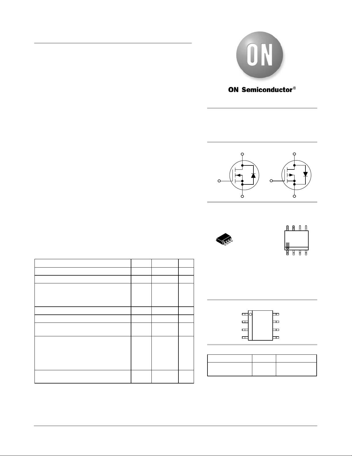
N−Source
1
2
3
4
8
7
6
5
N−Gate
P−Source
P−Gate
N−Drain
N−Drain
P−Drain
P−Drain
Device Package Shipping
†
ORDERING INFORMATION
N−Channel
D
S
G
PIN ASSIGNMENT
D
S
G
P−Channel
2 AMPERES, 30 VOLTS
R
DS(on)
= 70 mW (N-Channel)
R
DS(on)
= 200 mW (P-Channel)
http://onsemi.com
†For information on tape and reel specifications,
including part orientation and tape sizes, please
refer to our Tape and Reel Packaging Specification
Brochure, BRD8011/D.
MMDF2C03HDR2G SO−8
(Pb−Free)
2500 Tape & Reel
SO−8
CASE 751
STYLE 14
MARKING
DIAGRAM
D2C03 = Device Code
A = Assembly Location
Y = Year
WW = Work Week
G = Pb−Free Package
(Note: Microdot may be in either location)
D2C03
AYWWG
G
1
8
1
8
页面指南