
下载
© Semiconductor Components Industries, LLC, 2013
August, 2013 − Rev. 13
1 Publication Order Number:
MJD2955/D
MJD2955(PNP),
MJD3055(NPN)
Complementary Power
Transistors
DPAK for Surface Mount Applications
Designed for general purpose amplifier and low speed switching
applications.
Features
• Lead Formed for Surface Mount Applications in Plastic Sleeves
(No Suffix)
• Straight Lead Version in Plastic Sleeves (“−1” Suffix)
• Electrically Similar to MJE2955 and MJE3055
• High Current Gain−Bandwidth Product
• Epoxy Meets UL 94 V−0 @ 0.125 in
• NJV Prefix for Automotive and Other Applications Requiring
Unique Site and Control Change Requirements; AEC−Q101
Qualified and PPAP Capable
• These Devices are Pb−Free and are RoHS Compliant
MAXIMUM RATINGS
Rating Symbol Max Unit
Collector−Emitter Voltage V
CEO
60 Vdc
Collector−Base Voltage V
CB
70 Vdc
Emitter−Base Voltage V
EB
5 Vdc
Collector Current I
C
10 Adc
Base Current I
B
6 Adc
Total Power Dissipation
@ T
C
= 25°C
Derate above 25°C
P
D
{
20
0.16
W
W/°C
Total Power Dissipation (Note 1)
@ T
A
= 25°C
Derate above 25°C
P
D
1.75
0.014
W
W/°C
Operating and Storage Junction
Temperature Range
T
J
, T
stg
−55 to +150 °C
ESD − Human Body Model HBM 3B V
ESD − Machine Model MM C V
Stresses exceeding Maximum Ratings may damage the device. Maximum
Ratings are stress ratings only. Functional operation above the Recommended
Operating Conditions is not implied. Extended exposure to stresses above the
Recommended Operating Conditions may affect device reliability.
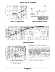
†Safe Area Curves are indicated by Figure 1. Both limits are applicable and must
be observed.
1. These ratings are applicable when surface mounted on the minimum pad
sizes recommended.
SILICON
POWER TRANSISTORS
10 AMPERES
60 VOLTS, 20 WATTS
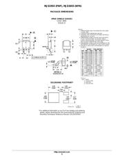
IPAK
CASE 369D
STYLE 1
DPAK
CASE 369C
STYLE 1
MARKING DIAGRAMS
AYWW
J
xx55G
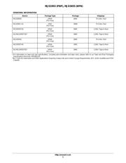
See detailed ordering and shipping information in the package
dimensions section on page 5 of this data sheet.
ORDERING INFORMATION
AYWW
J
xx55G
http://onsemi.com
A = Assembly Location
Y = Year
WW = Work Week
Jxx55 = Device Code
x = 29 or 30
G = Pb−Free Package
DPAK IPAK
1
2
3
4
1
2
3
4
COMPLEMENTARY
1
BASE
3
EMITTER
COLLECTOR
2, 4
1
BASE
3
EMITTER
COLLECTOR
2, 4
页面指南