
下载
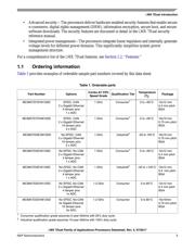
Ordering Information
See Table 1 on page 3
MCIMX7D
x
D
xxxxx
D
MCIMX7D
x
E
xxxxx
D
NXP Semiconductors
Data Sheet: Technical Data
Document Number: IMX7DCEC
Rev. 5, 07/2017
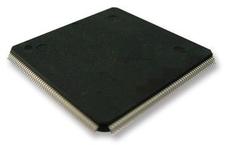
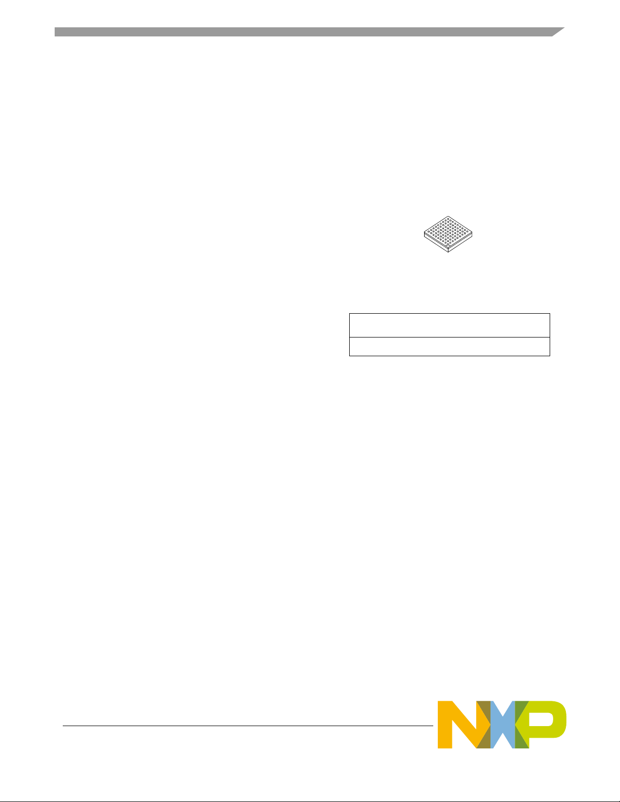
Package Information
Plastic Package
BGA 12 x 12 mm, 0.4 mm pitch
BGA 19 x 19 mm, 0.75 mm pitch
© 2016–2017 NXP B.V.
NXP reserves the right to change the detail specifications as may be required to permit improvements in the design of
its products.
1 i.MX 7Dual introduction
The i.MX 7Dual family of processors represents NXP’s
latest achievement in high-performance processing for
low-power requirements with a high degree of functional
integration. These processors are targeted towards the
growing market of connected and portable devices.
The i.MX 7Dual family of processors features advanced
implementation of the ARM
®
Cortex
®
-A7 core, which
operates at speeds of up to 1 GHz and 1.2 GHz,
depending on the part number. The i.MX 7Dual family
provides up to 32-bit
DDR3/DDR3L/LPDDR2/LPDDR3-1066 memory
interface and a number of other interfaces for connecting
peripherals, such as WLAN, Bluetooth, GPS, displays,
and camera sensors.
i.MX 7Dual Family of
Applications Processors
Datasheet
1 i.MX 7Solo introduction . . . . . . . . . . . . . . . . . . . . . . . . . . .1
1.1 Ordering information. . . . . . . . . . . . . . . . . . . . . . . . .3
1.2 Features . . . . . . . . . . . . . . . . . . . . . . . . . . . . . . . . . .4
2 Architectural overview . . . . . . . . . . . . . . . . . . . . . . . . . . . .8
2.1 Block diagram. . . . . . . . . . . . . . . . . . . . . . . . . . . . . .8
3 Modules list . . . . . . . . . . . . . . . . . . . . . . . . . . . . . . . . . . . .9
3.1 Special signal considerations . . . . . . . . . . . . . . . . .15
3.2 Recommended connections for unused analog
interfaces . . . . . . . . . . . . . . . . . . . . . . . . . . . . . . . .18
4 Electrical characteristics. . . . . . . . . . . . . . . . . . . . . . . . . .19
4.1 Chip-level conditions . . . . . . . . . . . . . . . . . . . . . . .19
4.2 Integrated LDO voltage regulator parameters . . . .34
4.3 PLL electrical characteristics . . . . . . . . . . . . . . . . .36
4.4 On-chip oscillators . . . . . . . . . . . . . . . . . . . . . . . . .36
4.5 I/O DC parameters . . . . . . . . . . . . . . . . . . . . . . . . .37
4.6 I/O AC parameters . . . . . . . . . . . . . . . . . . . . . . . . .41
4.7 Output buffer impedance parameters. . . . . . . . . . .45
4.8 System modules timing . . . . . . . . . . . . . . . . . . . . .47
4.9 General-purpose media interface (GPMI) timing . .67
4.10 External peripheral interface parameters . . . . . . . .75
4.11 12-Bit A/D converter (ADC) . . . . . . . . . . . . . . . . . 112
5 Boot mode configuration . . . . . . . . . . . . . . . . . . . . . . . . 113
5.1 Boot mode configuration pins. . . . . . . . . . . . . . . . 113
5.2 Boot device interface allocation . . . . . . . . . . . . . .114
6 Package information and contact assignments . . . . . . . 116
6.1 12 x 12 mm package information . . . . . . . . . . . . . 116
6.2 19 x 19 mm package information . . . . . . . . . . . . .134
7 Revision history . . . . . . . . . . . . . . . . . . . . . . . . . . . . . . .151
页面指南