

下载
MC100ES6111
Rev. 5, 07/2005
Freescale Semiconductor
Technical Data
© Freescale Semiconductor, Inc., 2005. All rights reserved.
Low Voltage 2.5/3.3 V Differential
ECL/PECL/HSTL Fanout Buffer
The MC100ES6111 is a bipolar monolithic differential clock fanout buffer.
Designed for most demanding clock distribution systems, the MC100ES6111
supports various applications that require distribution of precisely aligned
differential clock signals. Using SiGe:C technology and a fully differential
architecture, the device offers very low skew outputs and superior digital signal
characteristics. Target applications for this clock driver is high performance clock
distribution in computing, networking and telecommunication systems.
Features
• 1:10 differential clock distribution
• 35 ps maximum device skew
• Fully differential architecture from input to all outputs
• SiGe:C technology supports near-zero output skew
• Supports DC to 2.7 GHz operation of clock or data signals
• ECL/PECL compatible differential clock outputs
• ECL/PECL/HSTL compatible differential clock inputs
• Single 3.3 V, –3.3 V, 2.5 V or –2.5 V supply
• Standard 32-lead LQFP package
• 32-lead Pb-free package available
• Industrial temperature range
• Pin and function compatible to the MC100EP111
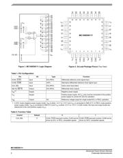
Functional Description
The MC100ES6111 is designed for low skew clock distribution systems and supports clock frequencies up to 2.7 GHz. The
device accepts two clock sources. The CLKA input can be driven by ECL or PECL compatible signals, the CLKB input accepts
HSTL compatible signals. The selected input signal is distributed to 10 identical, differential ECL/PECL outputs. If V
BB
is con-
nected to the CLKA input and bypassed to GND by a 10 nF capacitor, the MC100ES6111 can be driven by single-ended ECL/
PECL signals utilizing the V
BB
bias voltage output.
In order to meet the tight skew specification of the device, both outputs of a differential output pair should be terminated, even
if only one output is used. In the case where not all ten outputs are used, the output pairs on the same package side as the parts
being used on that side should be terminated.
The MC100ES6111 can be operated from a single 3.3 V or 2.5 V supply. As most other ECL compatible devices, the
MC100ES6111 supports positive (PECL) and negative (ECL) supplies. The MC100ES6111 is pin and function compatible to the
MC100EP111.
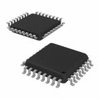
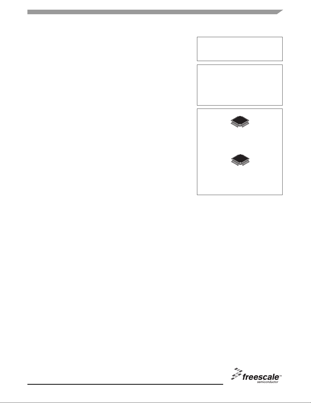
MC100ES6111
LOW-VOLTAGE 1:10 DIFFERENTIAL
ECL/PECL/HSTL
CLOCK FANOUT DRIVER
FA SUFFIX
32-LEAD LQFP PACKAGE
CASE 873A-04
AC SUFFIX
32-LEAD LQFP PACKAGE
Pb-FREE PACKAGE
CASE 873A-04