
下载
© Semiconductor Components Industries, LLC, 2009
June, 2009 − Rev. 2
1 Publication Order Number:
AN1596/D
AN1596/D
ECLinPS Lite™
Translator ELT Family
SPICE I/O Model Kit
Introduction
The objective of this kit is to provide customers with
enough schematic and SPICE parameter information to
perform system level interconnect modeling with the
ECLinPS Lite Translator ELT family. The ELT devices
MC10ELT2xD and MC100ELT2xD are single or dual
supply 1 or 2 Bit translators between the TTL and ECL
world. Single supply devices translate between TTL and
PECL, dual supply devices translate to or from negative
supplied ECL. All devices are designed as 100K compatible
100ELT2x or as 10H compatible 10ELT2x.
The family specifications are located in the High
Performance ECL Data book DL140/D. Section 3
represents the temperature and power supply variations that
can be expected from the family.
The kit contains representative schematics and model
files for the I/O circuits used by the ELT devices. In addition
a worst case package model schematic is included for more
accurate system level modeling. The package model should
be placed on all external inputs, outputs and supply pins.
This note includes the schematics necessary to do I/O
modeling and the model text−files.
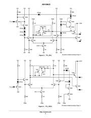
Input and Output Schematics
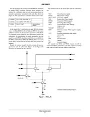
One schematic represents the PECL inputs of single
supply translators Figure 1, subcircuit PECL_IN. The
translation function of the dual supply
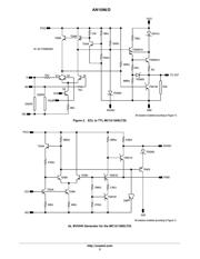
ECL−TTL−Translator MC10/100ELT25 is represented in
Figure 2 ECL_TTL_ELT25. This translator requires a
BVOHH reference signal. It is generated in the
BVOHH−generator (Figure 2a).
The TTL−(P)ECL Translator function uses separate
circuits for PECL and ECL outputs in 10ELT− or 100ELT
version shown in Figures 3 and 4 and subcircuits
TTL_ECL_100K, TTL_ECL_10H, TTL_PECL_100K,
TTL_PECL_10H.
The 10ELT and the 100ELT version of the (P)ECL outputs
are identical beside the temperature compensation network
included in the 100ELT−type output.
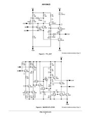
To simulate the TTL outputs the schematic Figure 5
TTL_OUT is used. The bias regulators ETXR, Figure 6 and
VCLP, Figure 7 are necessary to generate reference signals.
Replacing those subcircuits by voltage/current sources
would result in incorrect output modeling.
All inputs and outputs of the ELT family are protected by
ESD protection circuitry. The ESDPD subcircuit (Figure 8)
is used for ECL and PECL inputs. It contains ESD protection
and the standard ECL 75kΩ input pulldown resistors. The
ESD circuit of Figure 9 is used for TTL I/Os and the
ECL/PECL outputs.
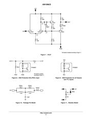
If the user would like to just simulate the output behavior
of an TTL output the TTL_OUT circuit can be stimulated
with internal signals.
To all external pins the package model PKG8 drawn in
Figure 10 needs to be added.
If users want to reduce simulation time and just simulate
1 channel or only the output of a circuit, they need to take
care of the correct power supply management. The channels
share power supply pins. Dynamic ICC current will add up
at power pins. When a simulation is performed with only one
channel, the package models of the power pins need to be
adjusted. The parasitic capacitance should be divided by two
and inductance should be doubled.
Modeling
The bias driver schematics for VBB and VCS generation
are not included in this kit, as they are unnecessary for
interconnection simulation. In addition their use would
result in a relatively large increase in simulation time.
Alternatively the internal reference voltages should be
driven with ideal constant voltage sources.
ÁÁÁÁÁÁ
ÁÁÁÁÁÁ
Parameter
ÁÁÁÁÁÁ
ÁÁÁÁÁÁ
Typical Level
ÁÁÁÁÁÁ
ÁÁÁÁÁÁ
Worst Case
ÁÁÁÁÁÁ
ÁÁÁÁÁÁ
VBB
ÁÁÁÁÁÁ
ÁÁÁÁÁÁ
VCC−1.325
ÁÁÁÁÁÁ
ÁÁÁÁÁÁ
Data Book
ÁÁÁÁÁÁ
ÁÁÁÁÁÁ
VCS
ÁÁÁÁÁÁ
ÁÁÁÁÁÁ
VEE+1.3V
ÁÁÁÁÁÁ
ÁÁÁÁÁÁ
±50mV
This model kit is intended for simulations within the
specified power supply range. If supply voltages drop below
minimum specification, VBB and VCS can no longer be
assumed to be constant. Thus this model kit can not been
used for power up or power down simulations.
http://onsemi.com
APPLICATION NOTE