
下载

Maxim > Design Support > Technical Documents > Application Notes > Analog Switches and Multiplexers > APP 2857
Maxim > Design Support > Technical Documents > Application Notes > T/E Carrier and Packetized > APP 2857
Keywords: T1, E1, J1, redundancy, analog switches, LIU, line interface unit, T1/E1/J1 line cards, N+1,
redundancy protection, transceivers
APPLICATION NOTE 2857
T1/E1/J1, N+1 Redundancy with Analog Switches
Dec 15, 2003
Abstract: Modern communications systems with multiport T1/E1/J1 line cards employ redundancy to
achieve the high-availability telecom networks require. Traditionally, these systems have used relays to
implement N+1 redundancy switching. As the number of T1/E1/J1 ports per line card and the number of
line cards per system increases, relays become impractical because of the board space and power they
require. Designers are using analog switches to replace relays. The advantages of analog switches over
relays include those listed in Table 1.
Related application note: Intel(R) T1/E1/J1, N+1 Redundancy With Analog Switches and Intel(R) LXT38x
Line Interface Units
Table 1. Analog Switches vs. Relays
Relay Analog Switch
Board Space 100mm² 15mm²
Power Consumption 140mW 5µW
Switching Speed 4ms 30ns
Reliability Mechanical Operation No Moving Parts
This application note shows how to implement T1/E1/J1, N+1 redundancy protection using analog
switches. It provides guidelines for selecting analog switches for your application and shows test results
using Maxim analog switches and T1/E1/J1 transceivers.
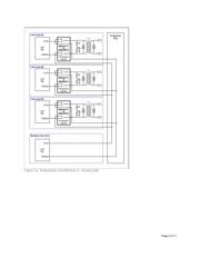
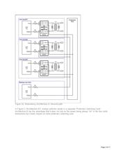
Redundancy Architectures
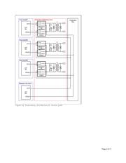
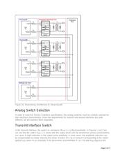
Figures 1 and 2 show two redundancy architectures with analog switches. For clarity, there are separate
drawings for the transmit and receive interfaces. Receive and transmit interfaces will reside in the same
board for each T1/E1 port. The drawings represent the typical interface transformers and resistors
recommended for a Maxim transceiver such as the DS2155. In both cases, there is a protection bus
running in the backplane where the input or output signals can be routed through the analog switches.
The protection bus connects directly to a backup (protection) line card.
In Figure 1 ("Architecture A"), analog switches reside in the line cards themselves. Architecture A has
the advantage of not requiring a separate line card for protection switching as in the "Architecture B"
below. It does require that the switches be powered even through fail-over switching which could require
a separate, dedicated power supply.
Page 1 of 11