

下载

Maxim > Design Support > Technical Documents > Application Notes > Amplifiers > APP 5129
Maxim > Design Support > Technical Documents > Application Notes > Sensors > APP 5129
Keywords: TIA, trans impedance amplifier, transimpedance amp, photodiode, medical instrumentation,
industrial control, piezo-sensor interface, TIA stability, feedback capacitance, phase compensation, bode plot
APPLICATION NOTE 5129
Stabilize Your Transimpedance Amplifier
By: Akshay Bhat, Senior Strategic Applications Engineer
Feb 03, 2012
Abstract: Transimpedance amplifiers (TIAs) are widely used to translate the current output of sensors like
photodiode-to-voltage signals, since many circuits and instruments can only accept voltage input. An
operational amplifier with a feedback resistor from output to the inverting input is the most straightforward
implementation of such a TIA. However, even this simple TIA circuit requires careful trade-offs among noise
gain, offset voltage, bandwidth, and stability. Clearly stability in a TIA is essential for good, reliable
performance. This application note explains the empirical calculations for assessing stability and then shows
how to fine-tune the selection of the feedback phase-compensation capacitor.
A similar version of this article appeared in the October 28, 2011 issue of Electronic Design magazine.
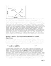
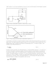
Wild Oscillations: Why Do They Happen?
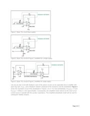
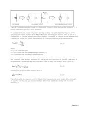
Figures 1 to 3 show some basic TIA circuits. Figure 1 is popularly used in dual-supply systems. Figure 2 is
a minor modification of this circuit for single-supply applications. The resistive-divider formed by R1 and R2
ensures that the output node of the op amp is higher than the Output Voltage Low specification during a
no-light condition when only a small dark current flows through the photodiode. By ensuring that the op
amp's output stage operates in the linear region, this offset improves both photo-detection in low-light
conditions and response speed. However, care must be taken to keep this bias voltage on the IN+ pin
small. Otherwise reverse-leakage current in the photodiode can degrade linearity and increase offset drift
over temperature. In some applications the circuit in Figure 3 is used where the photodiode is placed
directly across the input terminals of the op amp. This circuit avoids the reverse bias across the photodiode,
although it requires a buffered reference. The reference must be fast enough to sink the photodiode current
as required by the application. This, in turn, implies that amplifier A1 must be as fast as amplifier A2.
Page 1 of 11