
下载
© Semiconductor Components Industries, LLC, 2013
December, 2013 − Rev. 1
1 Publication Order Number:
AND9129/D
AND9129/D
Understanding a Digital
Transistor Datasheet
Introduction
This application note will describe the common
specifications of a Digital Transistor. It will also show how
to use these specifications to successfully design with a
Digital Transistor. Parameters from the DTC114E/D
datasheet will be used to help with explanations. This
datasheet describes a Digital Transistor that has an input
resistor, R1, equal to 10 kW and a base−emitter resistor, R2,
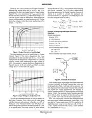
equal to 10 kW. Figure 1 gives a labeled schematic of a
Digital Transistor. These labels will be used throughout this
application note.
Figure 1. Labeled Schematic
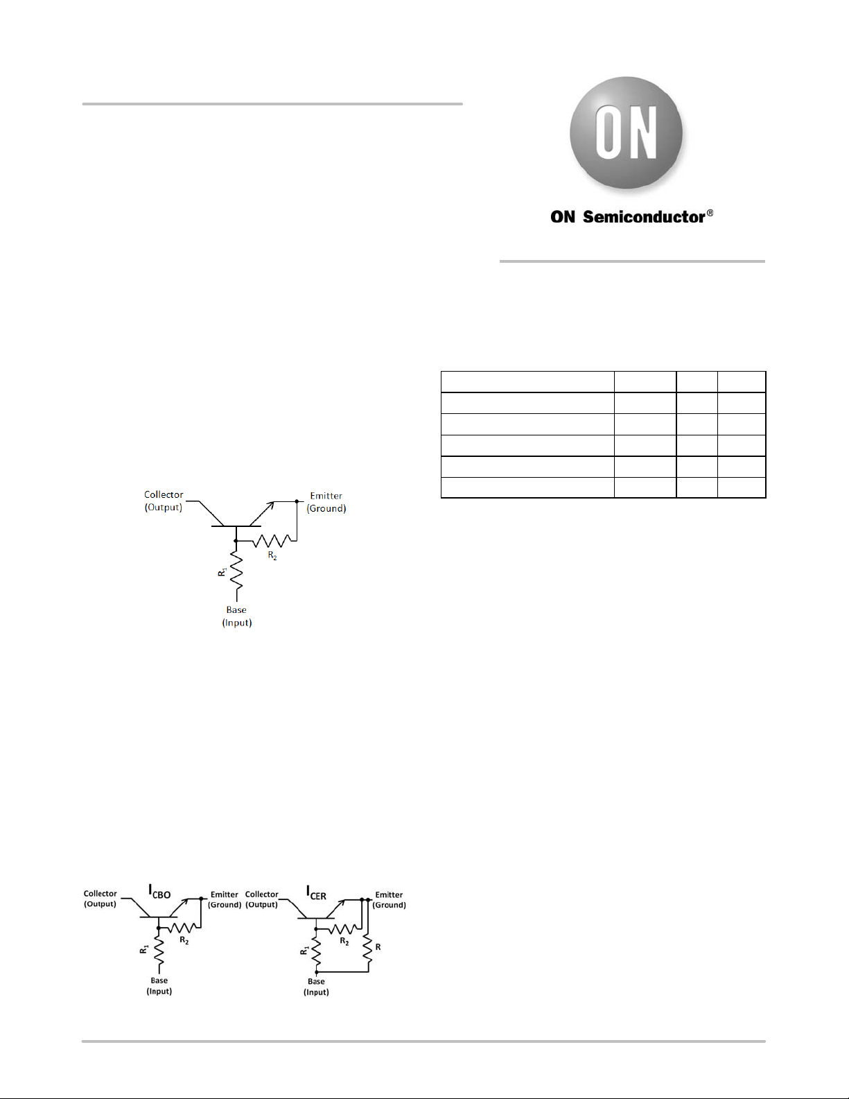
For Digital Transistors it is important to realize that the
transistor and resistor network is considered as one unit. An
example of this is the I
CBO
parameter. Looking at this
parameter one would think that it is not possible. How could
the emitter be open when R
2
connects the emitter and base
of the transistor? Shouldn’t it be I
CER
? The answer is yes R
2
connects the emitter and base of the transistor, but this
connection is built into the device. What is considered the
emitter and base of the Digital Transistor is left open. In the
case of a Digital Transistor I
CER
would mean that there is an
additional resistor placed between the emitter and base of the
digital transistor. Figure 2 shows the difference between
I
CBO
and I
CER
when referring to Digital Transistors.
Figure 2. I
CBO
vs. I
CER
Maximum Ratings
Below is the maximum ratings table that can be found in
every Digital Transistor datasheet.
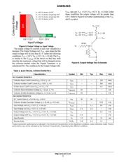
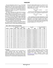
Table 1. MAXIMUM RATINGS
Rating Symbol Max Unit
Collector−Base Voltage V
CBO
50 Vdc
Collector−Emitter Voltage V
CEO
50 Vdc
Collector Current – Continuous I
C
100 mAdc
Input Forward Voltage V
IN(fwd)
40 Vdc
Input Reverse Voltage V
IN(rev)
10 Vdc
Stresses exceeding those listed in the Maximum Ratings table
may damage the device. If any of these limits are exceeded,
device functionality should not be assumed, damage may occur
and reliability may be affected.
The first spec, V
CBO
, states that the maximum voltage that
can be applied from the collector to the base is 50 V. The
Collector−Emitter Voltage, V
CEO
, spec states the maximum
voltage that can be applied from the collector to emitter is
50 V. In addition, the table specifies that the maximum DC
collector current (I
C
) that the device can conduct is 100 mA.
There are two maximum ratings for the input voltage,
forward and reverse. The input voltage is defined as the
voltage applied from the base and the emitter. The maximum
input forward voltage is determined from the power
capabilities of the input resistor, R
1
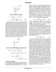
. Figure 3 and Equations
1 and 2 describe how the maximum input forward voltage is
calculated when the maximum power capability of R
1
is
220 mW. It is important to use the minimum value of R
1
because it will cause the greatest power to be dissipated on the
die. The minimum value of R
1
can be found in the Electrical
Characteristics Table of every Digital Transistor datasheet. In
this case R
1(min)
= 7 kW. The resulting maximum input
forward voltage is 40 V. For this particular device a voltage
greater than this would result in the resistor failing.
APPLICATION NOTE
http://onsemi.com