


下载

Maxim > Design Support > Technical Documents > Application Notes > Temperature Sensors and Thermal Management > APP 5727
Keywords: temperature sensor, I2C slave addressing, multidrop
APPLICATION NOTE 5727
Understanding Multidrop Address Assignments for
Thermal Sensors
Mar 28, 2014
Abstract:
In
many thermal applications, it may be desired to utilize multiple temperature sensors, placed in
different physical locations, to monitor the operating temperatures in predefined 'zones' within the system. To
accommodate this desire, many thermal products have the added flexibility of user-defined slave addressing.
A similar version was published in the March 2014 issue of Electronics Maker magazine.
Traditionally, most ICs incorporating the Philips
®
I
2
C I/O protocol have a fixed (factory-defined) slave address
for use during communications. In many thermal applications, however, it may be desirable to utilize multiple
temperature sensors, placed in different physical locations, to monitor the operating temperatures in predefined
"zones" within the system. To accommodate this while minimizing CPU resources allocated for
communications functions, many thermal products have the added flexibility of user-defined slave addressing.
This user-defined function uses an additional input pin (or pins) that allows mapping of a specific sensor to a
schematically defined slave address.
Categorizing the thermal products by its I/O multidrop capability results in three fundamental variations of the
options for user-defined slave addressing:
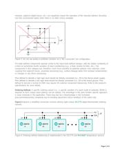
Input-Level Defined. The condition of the address input pin can be controlled by a simple hardware definition
(i.e., resistor placement) or by a dynamic CPU resource. Standard digital logic input levels (V
IH
/V
IL
) utilized on
SCL and SDA can also be applied to the address input pin(s).
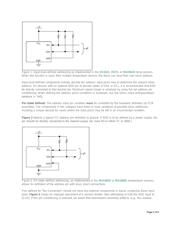
Figure 1 depicts a typical I
2
C resistor pullup scheme where the I
2
C master's resource is defined as open
drain, and the default ADD pin state is Logic 1. The desired decode (ADD input bias) must be presented prior
to the associated START signal whenever this slave is to be accessed; it should remain stable until after the
associated STOP has been issued.
Page 1 of 6