
下载
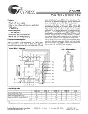
256K(32K x 8) Static RAM
CY7C1399B
Cypress Semiconductor Corporation • 3901 North First Street • San Jose, CA 95134 • 408-943-2600
Document #: 38-05071 Rev. *D Revised July 11, 2005
Features
• Single 3.3V power supply
• Ideal for low-voltage cache memory applications
•High speed
— 10/12/15 ns
• Low active power
— 216 mW (max.)
• Low-power alpha immune 6T cell
• Plastic SOJ and TSOP packaging
Functional Description
[1]
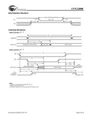
The CY7C1399B is a high-performance 3.3V CMOS Static
RAM organized as 32,768 words by 8 bits. Easy memory
expansion is provided by an active LOW Chip Enable (CE
) and
active LOW Output Enable (OE
) and three-state drivers. The
device has an automatic power-down feature, reducing the
power consumption by more than 95% when deselected.
An active LOW Write Enable signal (WE
) controls the
writing/reading operation of the memory. When CE
and WE
inputs are both LOW, data on the eight data input/output pins
(I/O
0
through I/O
7
) is written into the memory location
addressed by the address present on the address pins (A
0
through A
14
). Reading the device is accomplished by selecting
the device and enabling the outputs, CE
and OE active LOW,
while WE
remains inactive or HIGH. Under these conditions,
the contents of the location addressed by the information on
address pins is present on the eight data input/output pins.
The input/output pins remain in a high-impedance state unless
the chip is selected, outputs are enabled, and Write Enable
(WE
) is HIGH. The CY7C1399B is available in 28-pin standard
300-mil-wide SOJ and TSOP Type I packages.
Note:
1. For guidelines on SRAM system design, please refer to the ‘System Design Guidelines’ Cypress application note, available on the internet at www.cypress.com.
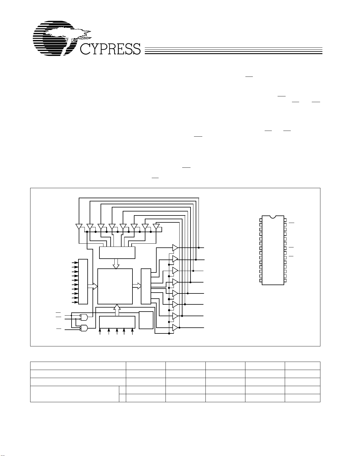
Logic Block Diagram
Pin Configurations
1
2
3
4
5
6
7
8
9
10
11
14
15
16
20
19
18
17
21
24
23
22
Top View
SOJ
12
13
25
28
27
26
GND
A
6
A
7
A
8
A
9
A
10
A
11
A
12
A
13
WE
V
CC
A
4
A
3
A
2
A
1
I/O
7
I/O
6
I/O
5
I/O
4
A
14
A
5
I/O
0
I/O
1
I/O
2
CE
OE
A
0
I/O
3
A
1
A
2
A
3
A
4
A
5
A
6
A
7
A
8
COLUMN
DECODER
ROW DECODER
SENSE AMPS
INPUT BUFFER
POWER
DOWN
WE
OE
I/O
0
CE
I/O
1
I/O
2
I/O
3
32K x 8
ARRAY
I/O
7
I/O
6
I/O
5
I/O
4
A
9
A
0
A
11
A
13
A
12
A
14
A
10
Selection Guide
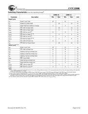
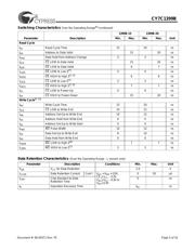
1399B-10 1399B-12 1399B-15 1399B-20 Unit
Maximum Access Time 10 12 15 20 ns
Maximum Operating Current 60 55 50 45 mA
Maximum CMOS Standby Current 500 500 500 500 µA
L50
50 50 50 µA