
下载
Publication Order Number:
BAT54WT1/D
Semiconductor Components Industries, LLC, 2011
November, 2011 − Rev. 10
1
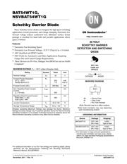
BAT54WT1G,
NSVBAT54WT1G
Schottky Barrier Diode
These Schottky barrier diodes are designed for high speed switching
applications, circuit protection, and voltage clamping. Extremely low
forward voltage reduces conduction loss. Miniature surface mount
package is excellent for hand held and portable applications where
space is limited.
Features
Extremely Fast Switching Speed
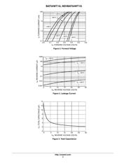
Extremely Low Forward Voltage − 0.35 V (Typ) @ I
F
= 10 mAdc
AEC Qualified and PPAP Capable
NSV Prefix for Automotive and Other Applications Requiring
Unique Site and Control Change Requirements
These Devices are Pb−Free, Halogen Free/BFR Free and are RoHS
Compliant*
MAXIMUM RATINGS (T
J
= 125C unless otherwise noted)
Rating
Symbol Value Unit
Reverse Voltage V
R
30 V
Forward Power Dissipation
@ T
A
= 25C
Derate above 25C
P
F
200
1.6
mW
mW/C
Forward Current (DC) I
F
200 Max mA
Non−Repetitive Peak Forward
Current,
t
p
< 10 msec
I
FSM
600
mA
Repetitive Peak Forward Current
Pulse Wave = 1 sec,
Duty Cycle = 66%
I
FRM
300
mA
Junction Temperature T
J
−55 to 125 C
Storage Temperature Range T
stg
−55 to +150 C
Stresses exceeding Maximum Ratings may damage the device. Maximum
Ratings are stress ratings only. Functional operation above the Recommended
Operating Conditions is not implied. Extended exposure to stresses above the
Recommended Operating Conditions may affect device reliability.
*For additional information on our Pb−Free strategy and soldering details, please
download the ON Semiconductor Soldering and Mounting Techniques
Reference Manual, SOLDERRM/D.
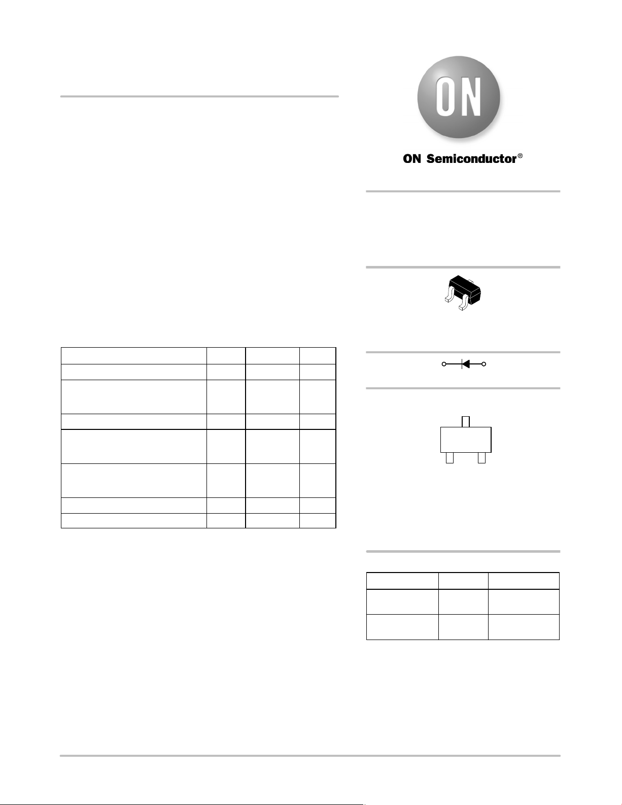
3
CATHODE
1
ANODE
30 VOLT
SCHOTTKY BARRIER
DETECTOR AND SWITCHING
DIODE
†For information on tape and reel specifications,
including part orientation and tape sizes, please
refer to our Tape and Reel Packaging Specifications
Brochure, BRD8011/D.
Device Package Shipping
†
ORDERING INFORMATION
BAT54WT1G SOT−323
(Pb−Free)
3,000 /
Tape & Reel
http://onsemi.com
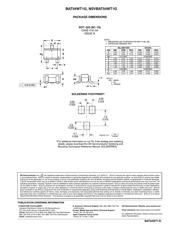
SOT−323
CASE 419
STYLE 2
MARKING DIAGRAM
B4M G
G
B4 = Device Code
M = Date Code*
G = Pb−Free Package
(Note: Microdot may be in either location)
*Date Code orientation may vary depending
upon manufacturing location.
1
NSVBAT54WT1G SOT−323
(Pb−Free)
3,000 /
Tape & Reel