
下载

Atmel AVR211: Wafer Level Chip Scale Packages
Features
• Allows integration using the smallest possible form factor
– Packaged devices are practically the same size as the die
• Small footprint and package height
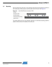
• Low inductance between die and PCB
• High thermal conduction characteristics
• Short manufacturing cycle time
• Light-weight: no leadframe, mold compound or substrate
1. Introduction
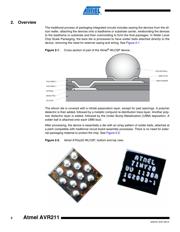
Wafer Level Chip Scale Packaging (WLCSP) refers to the technology of packaging an
integrated circuit at wafer level, resulting in a device practically the same size as the
die. While the name implies devices would be packaged the bare die is actually modi-
fied to add environmental protection layers and solder balls that are then used as the
direct connection to the package carrier or substrate. WLCSP technology allow
devices to be integrated in the design using the smallest possible form factor. WLCSP
devices require no additional process steps on surface mount assembly lines.
Figure 1-1. Size comparison (largest to smallest): DIP, VQFN, SOT, and WLCSP.
8-bit Atmel
Microcontrollers
Application Note
Rev. 42007A–AVR–06/12