
下载

© Semiconductor Components Industries, LLC, 2016
December, 2017 − Rev. 9
1 Publication Order Number:
AN52561/D
AN52561/D
Image Sensor Handling and
Best Practices
Application Note Abstract
This application note describes methods for handling,
storing, and cleaning image sensors.
INTRODUCTION
Integrated circuits, including image sensor products are
sensitive to Electrostatic Discharge (ESD).
ESD events can cause immediate damage to a device so
that it is no longer functional. The effect may also not be
noticed until a considerable time has passed, with the unit
operating to specifications for some time. ESD events also
show up as shifts in device characteristics.
ESD events occur by improper handling of the image
sensor. Improper handling includes any operation that
creates an electrostatic discharge; for example, handling the
device without a wrist strap. Environmental conditions also
contribute to the likelihood of ESD event.
The cost of an appropriate ESD control program is well
offset by the savings achieved in avoiding damaged devices
(see References [1] and [2]).
This application note discusses some recommended
procedures to minimize the occurrence of an ESD event
when handling image sensors. The recommendations in this
application note follow JEDEC Standard JESD625-A.
ON Semiconductor recommends that our customers
become familiar with and follow the procedures in JEDEC
Standard JESD625-A3.
Disclaimer
ON Semiconductor is not responsible for damage caused
by improper handling or cleaning of the device after it is
received by the customer.
Rating
ON Semiconductor CMOS image sensors, unless stated
otherwise in the applicable device datasheet, are rated as
follows for ESD sensitivity according to the JESD22
classification method:
• Human Body Model: JS001−2013 Class2
• Charged Device Model: JESD22−C101 Class III [4]
NOTE: For CCD devices, unless a JESD22 rating is
specified, consider the product to meet Class 0
or A rating.
Glossary of Terms and Definitions
For the purpose of this application note, the following
definitions apply:
• Air Ionizer: A source of charged air molecules (ions).
• Antistatic Material: Refers to the property of material
that inhibits tribo-electric charging.
• Conductive Material: A material that has a surface
resistivity less than 10
5
per square or a volume
resistivity less than 10
4
centimeter.
• Electrostatic Discharge (ESD): The transfer of
electrostatic charge between bodies or surfaces that are
at different electrostatic potentials.
• Electrostatic Discharge Susceptibility [sensitivity]
(ESDS): The lowest level of ESD that produces changes
in device characteristics such that the device fails to
meet its specified characteristics.
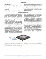
• ESD-Protective Packaging: A packaging system that
provides electrostatic protection and limits
tribo-electric charging to levels that do not result in
device damage.
• ESD-Protective Work-Surface: A table top or other
surface on which to work that has a resistance to
ground of less than 10
9
.
• Insulation Material: A material having a surface
resistivity of at least 10
12
per square or volume
resistivity of at least 10
11
centimeter.
• Static Dissipative Material: A material having a surface
resistance between 10
5
and 10
8
or a volume
resistivity between 10
5
centimeters and 10
8
centimeters.
• Static Electricity: Electrical charge at rest.
The electrical charge is due to the transfer of electrons
within a body (polarization) or from one body to
another.
www.onsemi.com
APPLICATION NOTE