
下载
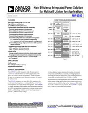
High Efficiency Integrated Power Solution
for Multicell Lithium Ion Applications
Data Sheet
ADP5080
FEATURES
Wide input voltage range: 4.0 V to 15 V
High efficiency architecture
Up to 2 MHz switching frequency
6 synchronous rectification dc-to-dc converters
Channel 1 buck regulator: 3 A maximum
Channel 2 buck regulator: 1.15 A maximum
Channel 3 buck regulator: 1.5 A maximum
Channel 4 buck regulator: 0.8 A maximum
Channel 5 buck regulator: 2 A maximum
Channel 6 configurable buck or buck boost regulator
2 A maximum for buck regulator configuration
1.5 A maximum for buck boost regulator configuration
Channel 7 high voltage, high performance LDO regulator:
30 mA maximum
2 low quiescent current keep-alive LDO regulators
LDO1 regulator: 400 mA maximum
LDO2 regulator: 300 mA maximum
Control circuit
Charge pump for internal switching driver power supply
I
2
C-programmable output levels and power sequencing
Package: 72-ball, 4.5 mm × 4.0 mm × 0.6 mm WLCSP
(0.5 mm pitch)
APPLICATIONS
DSLR cameras
Non-reflex (mirrorless) cameras
Portable instrumentation
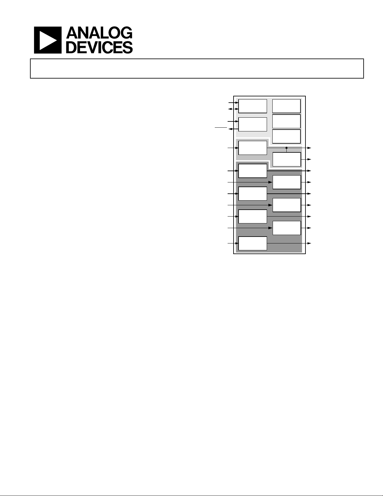
FUNCTIONAL BLOCK DIAGRAM
Figure 1.
GENERAL DESCRIPTION
The ADP5080 is a fully integrated, high efficiency power
solution for multicell lithium ion battery applications. The
device can connect directly to the battery, which eliminates
the need for preregulators and, therefore, increases the battery
life of the system.
The ADP5080 integrates two keep-alive LDO regulators, five
synchronous buck regulators, a configurable four-switch buck
boost regulator, and a high voltage LDO regulator. The ADP5080
is a highly integrated power solution that incorporates all power
MOSFETs, feedback loop compensation, voltage setting resistor
dividers, and discharge switches, as well as a charge pump to
generate a global bootstrap voltage.
All these features help to minimize the number of external
components and PCB space required, providing significant
advantages for portable applications. The switching frequency
is selectable on each channel from 750 kHz to 2 MHz.
Key functions for power applications, such as soft start, selectable
preset output voltage, and flexible power-up and power-down
sequences, are provided on chip and are programmable via the
I
2
C interface with fused factory defaults. The ADP5080 is available
in a 72-ball WLCSP 0.5 mm pitch package.
LDO1
LDO2
I
2
C
INTERFACE
CONTROL
LOGIC
OSCILLATOR
VOLTAGE
REFERENCE
SCL
SDA
ENABLE
3V TO 3.3V, 300mA
1.0V TO 3.3V, 1.15A
CH1 BUCK
REGULATOR
0.80V TO 1.20V, 3A
5.0V TO 5.5V, 400mA
CHARGE
PUMP
1.2V TO 1.8V/ADJ, 1.5A
1.8V TO 3.55V/ADJ, 0.8A
3.0V TO 5.0V, 2A
3.5V TO 5.5V/ADJ
BUCK ONLY: 2A
BUCK BOOST: 1.5A
5V TO 12V, 30mA
11639-001
FAULT
4V TO 15V
4V TO 15V
5V TO 25V
4V TO 15V
4V TO 15V
4V TO 15V
4V TO 15V
4V TO 15V
CH 3 BUCK
REGULATOR
CH2 BUCK
REGULATOR
CH 4 BUCK
REGULATOR
CH 6
BUCK BOOST
REGULATOR
CH 5 BUCK
REGULATOR
CH7 LDO
REGULATOR
Rev. A Document Feedback
Information furnished by Analog Devices is believed to be accurate and reliable. However, no
responsibility is assumed by Analog Devices for its use, nor for any infringements of patents or other
rights of third parties that may result from its use. Specifications subject to change without notice. No
license is granted by implication or otherwise under any patent or patent rights of Analog Devices.
Trademarks and registered trademarks are the property of their respective owners.
One Technology Way, P.O. Box 9106, Norwood, MA 02062-9106, U.S.A.
Tel: 781.329.4700 ©2013–2014 Analog Devices, Inc. All rights reserved.
Technical Support www.analog.com
页面指南