
下载
Analog Dialogue 36-03 (2002) 1
Ask the Applications Engineer—30
by Adrian Fox [adrian.fox@analog.com]
PLL SYNTHESIZERS
Q. What is a PLL Synthesizer?
A. A frequency synthesizer allows the designer to generate a variety of
output frequencies as multiples of a single reference frequency.
The main application is in generating local oscillator (LO)
signals for the up- and down-conversion of RF signals.
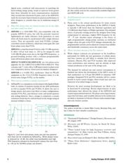
The synthesizer works in a phase-locked loop (PLL), where
a phase/frequency detector (PFD) compares a fed back
frequency with a divided-down version of the reference
frequency (Figure 1). The PFD’s output current pulses are
ltered and integrated to generate a voltage. This voltage drives
an external voltage-controlled oscillator (VCO) to increase or
decrease the output frequency so as to drive the PFD’s average
output towards zero.
Frequency is scaled by the use of counters. In the example
shown, an ADF4xxx synthesizer is used with an external lter
and VCO. An input reference (R) counter reduces the reference
input frequency (13 MHz in this example) to PFD frequency
(F
PFD
= F
REF
/R); and a feedback (N) counter reduces the
output frequency for comparison with the scaled reference
frequency at the PFD. At equilibrium, the two frequencies
are equal, and the output frequency is N F
PFD
. The
feedback counter is a dual-modulus prescaler type, with A and B
counters (N = BP + A, where P is the prescale value).
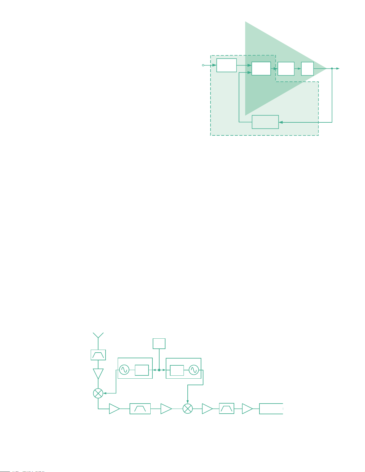
Figure 2 shows a typical application in a superheterodyne
receiver. Base station and handset LOs are the most common
application, but synthesizers are also found in low frequency
clock generators (ADF4001), wireless LANs (5.8 GHz), radar
systems, and collision-avoidance systems (ADF4106).
Q. What are the key performance parameters to be considered in selecting
a PLL synthesizer?
A. The major ones are: phase noise, reference spurs, and
lock time.
Phase Noise: For a carrier frequency at a given power level,
the phase noise of a synthesizer is the ratio of the carrier power
to the power found in a 1-Hz bandwidth at a de ned frequency
offset (usually 1 kHz for a synthesizer). Expressed in dBc/Hz,
the in-band (or close-in) phase noise is dominated by the
synthesizer; the VCO noise contribution is high-pass ltered
in the closed loop.
Reference Spurs: These are artifacts at discrete offset
frequencies generated by the internal counters and charge
pump operation at the PFD frequency. These spurs will
be increased by mismatched up and down currents from
the charge pump, charge-pump leakage, and inadequate
decoupling of supplies. The spurious tones will get mixed down
on top of the wanted signal and decrease receiver sensitivity.
Lock Time: The lock time of a PLL is the time it takes to jump
from one speci ed frequency to another speci ed frequency
within a given frequency tolerance. The jump size is normally
determined by the maximum jump the PLL will have to
accomplish when operating in its allocated frequency band.
The step-size for GSM-900 is 45 MHz and for GSM-1800
is 95 MHz. The required frequency tolerances are 90 Hz and
180 Hz, respectively. The PLL must complete the required
frequency step in less than 1.5 time slots, where each time
slot is 577 µs.
All trademarks and registered trademarks are the property of their respective holders.
Figure 2. Dual PLL used to mix down from GSM RF to baseband.
�
�
�
Figure 1. Block diagram of a PLL.