
下载
Safe Harbor Statement
This publication contains forward-looking statements that involve a number of risks and uncertainties. These "forward-
looking statements" are intended to qualify for the safe harbor from liability established by the Private Securities Litigation
Reform Act of 1995. These forward-looking statements generally can be identified by phrases such as TI or its management
"believes," "expects," "anticipates," "foresees," "forecasts," "estimates" or other words or phrases of similar import.
Similarly, such statements herein that describe the company's products, business strategy, outlook, objectives, plans,
intentions or goals also are forward-looking statements. All such forward-looking statements are subject to certain risks
and uncertainties that could cause actual results to differ materially from those in forward-looking statements. Please refer
to TI's most recent Form 10-K for more information on the risks and uncertainties that could materially affect future results
of operations. We disclaim any intention or obligation to update any forward-looking statements as a result of
developments occurring after the date of this publication.
SCYB012
Reliable. Logic. Innovation.; the red/black banner; NanoStar
and NanoFree are trademarks of Texas Instruments.
© 2003 Texas Instruments Incorporated
For More Information
Product Folder:
www.ti.com/sc/device/sn74avca164245
www.ti.com/sc/device/sn74avcb164245
Data Sheet:
www-s.ti.com/sc/techlit/sces395
www-s.ti.com/sc/techlit/sces394
Application Note:
www-s.ti.com/sc/techlit/scea030
Translation Homepage:
www.ti.com/trans
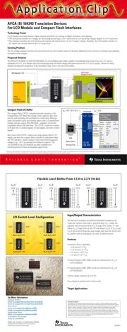
Flexible Level Shifter From 1.5 V to 3.3 V (16-bit)Flexible Level Shifter From 1.5 V to 3.3 V (16-bit)
AVCB164245
AVCA164245
1.5 V
V
CC
B
3.3 V
1.5 V
V
CC
A
3.3 V
AVCB164245
AVCA164245
1.5 V
V
CC
B
3.3 V
1.8 V
V
CC
A
3.3 V
AVCB164245
AVCA164245
1.5 V
V
CC
B V
CC
A
3.3 V
2.5 V
3.3 V
Input/Output Characteristics
The SN74AVCA164245 and SN74AVCB164245 translators are
“split-rail” devices. One side is powered from V
CC
A while the
opposite side is powered from V
CC
B. Logic I/O’s on the “A” side
follow V
CC
A. Logic I/O’s on the “B” side follow V
CC
B. If V
CC
A and
V
CC
B are powered from the same supply rail, then the device acts
as a buffer with no translation. In total, 16 different level
Features
•
Dynamic Drive Capability
- ± 24 mA at 3 V V
CC
- ± 15 mA at 2.3 V V
CC
- ± 9 mA at 1.65 V V
CC
- ± 6 mA at 1.4 V V
CC
•
Control Inputs (DIR, OE#) levels are referenced to V
CC
A
(AVCA164245)
•
Control Inputs (DIR, OE#) levels are referenced to V
CC
B
(AVCB164245)
•
Over-voltage tolerant up to 3.6 V
•
I
off
supports partial power down mode
Target Applications
I/O Switch Level ConfigurationI/O Switch Level Configuration
V
CC
B, V
CC
A = 3.3 V
AVCB164245
AVCA164245
3.3 V3.3 V
V
CC
B, V
CC
A = 1.8 V
AVCB164245
AVCA164245
1.8 V1.8 V
V
CC
B, V
CC
A = 2.5 V
AVCB164245
AVCA164245
2.5 V2.5 V
V
CC
B, V
CC
A = 1.5 V
AVCB164245
AVCA164245
1.5 V1.5 V
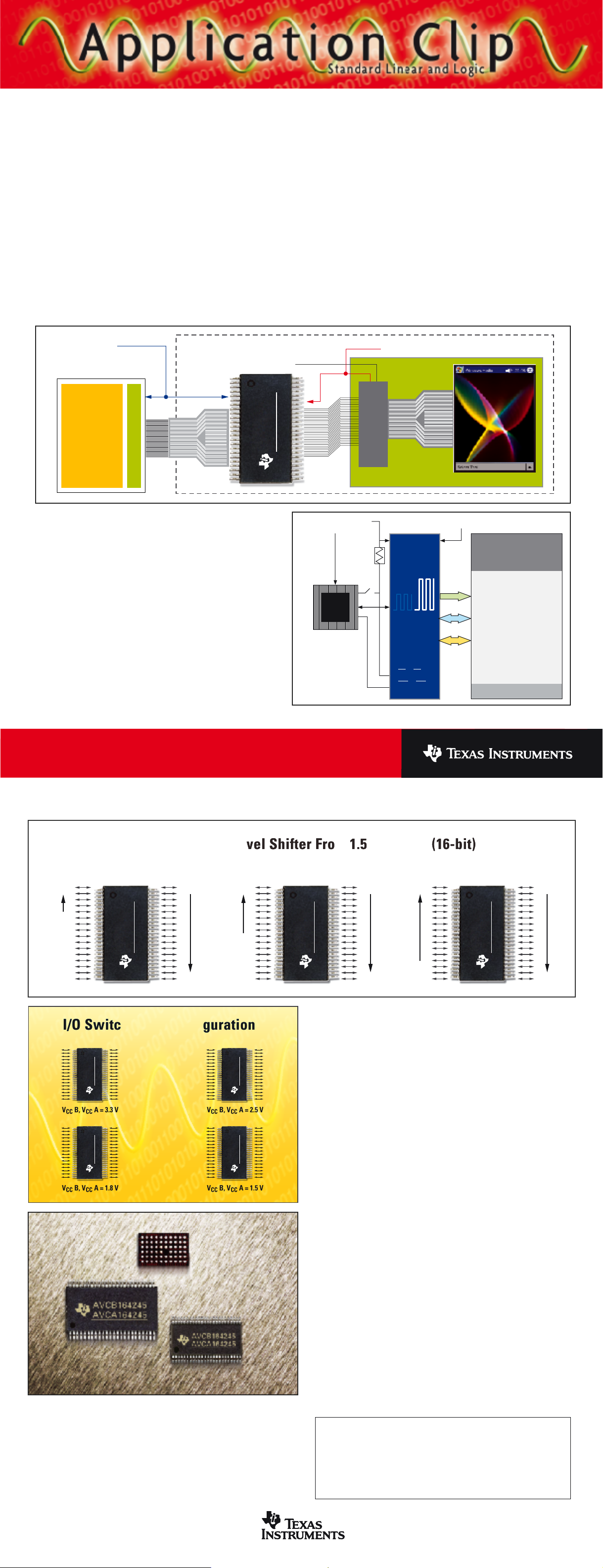
LFBGA
TSSOP
TVSOP
AVCB164245
AVCA164245
AVCA (B) 164245 Translation Devices
For LCD Module and Compact Flash Interfaces
Technology Trend
•
LCD displays on mobile phones, digital cameras and PDA's are moving to higher-resolution color displays.
•
CPU and microcontroller I/O voltages are decreasing and moving to 2.5-V and below as core operating voltages migrate to 1.8-V and lower.
•
The existing controllers for LCD panels in the market still operate from 3 to 3.6-V supply voltages. Similarly, the LCD module interface in
the market also remains fixed at the 3.3-V logic level.
Existing Problem
The I/O voltage mismatch between the processor and the LCD module makes it extremely difficult for these devices to interface and maintain
acceptable noise margins.
Proposed Solution
The SN74AVCA164245 (or SN74AVCB164245) is a level-shifting logic buffer capable of translating from levels as low as 1.4-V up to a
maximum of 3.6-V. It is ideally suited for interfacing with the lower-voltage microprocessor to the 3.3-V LCD module. Below is a block
diagram showing the integration of the translation logic device onto the LCD module.
Compact Flash I/O Buffer
The compact flash (CF/CF+) standard provides interface to the
CompactFlash (CF) flash data storage cards, magnetic disk cards
and I/O cards including, but not limited to, serial cards, Ethernet
cards, fax/modem cards, and wireless pager cards. A CompactFlash
storage card also runs in True IDE Mode – making it electrically
compatible with an IDE disk drive. The CF/CF+ connector consists
of 50 pins with 11 address signals, 16 data signals, and other control
signals.
Since most of the CF/CF+ cards in use today operate with a 3.3 V
supply, and since the compact flash controller is embedded within
the CPU and MCU, which is subject to the trend of decreasing I/O
voltages (e.g., 1.8V), an external level shifter is required. The
AVCA164245 or the AVCB164245 are ideal candidates for
interfacing between these incompatible signal levels.
•
Memory Mode
•
I / O Mode
•
True IDE Mode
Inputs Outputs I / O
A10~A0 CD1~2 BVD1~2
CE1~2 INPACK
CSEL RDY D15~D0
OE VS1~2
REG Wait
RESET WP
WE
IORead
IOWrite
20-bits 8-bits 18-bits
V
cc
= 3.3 V
V
IN
= 1.5 V / 1.8 V / 2.5 V V
IN
= 3.3 V
AVCB164245
V
CC
B
1.8 V 3.3 V
Address
Data
Controls
1OE, 2OE
1DIR, 2DIR
V
CC
A
Chipset
PDA
Digital Camera
Wireless Chip
Memory
I / F
Embedded CPU
LDO Regulator 1.8 V
• PDA
• Cellular
• Digital Camera
Analog Power
Current LCD Module
LCD Interface
Logic Power
Voltage (2.3-3.6 V)
TI bears no responsibility for problems that may arise with third party rights, including intellectual property rights, in connection with use of the information contained in this document. The Material on this document
are provided for information purpose only. TI assumes no liability for applications assistance or customer product design.
LCD Controller
R
ELIABLE
.
L
OGIC.
I
NNOVATION
.
™